

Deep ultraviolet (DUV) light emitting diodes (LED) made of Aluminium Gallium Nitride (AlGaN) are increasingly considered as light sources for medical as well as material processing applications. Recent research on AlGaN DUV LEDs focuses on the enhancement of the efficiency. The efficiency of AlGaN LEDs is limited by a low hole injection efficiency and TM-polarized […]
MM03–Comparison of Scharfetter-Gummel Schemes for (Non-)Degenerate Semiconductor Device Simulation
We consider Voronoi finite volume schemes for the discretization of the van Roosbroeck system and pay particular attention to the choice of flux approximations. The classical Scharfetter-Gummel scheme yields a thermodynamically consistent numerical flux, but cannot be used for general charge carrier statistics.We compare and analyze aspects of two state-of-the-art modified Scharfetter-Gummel schemes to simulate […]
LD05–Optical Design Issues in Electrically Pumped Tunable Liquid-Crystal VCSELs
In this work we investigate a tunable 850nm laser based on a hybrid combination of a liquid crystal micro-cell and a half GaAs VCSEL. The target application is optical coherence tomography. The inherent tolerances of the hybrid technology, the presence of metals in the cavity and the need for a pure extraordinary mode lasing make […]
N04–Silicon-Integrated Red-Light Optical Gain Medium Based on BGaAs/GaP Quantum Wells
In this study we present BGaAs/GaP quantum well (QW) structures integrated with GaP/Si virtual substrate as a promising structure for applications requiring red-light optical gain media. Gain spectra are computed based on an 8-band k · p model with an envelope function approximation and Fermi’s Golden Rule. An emission of red light of wavelengths from […]
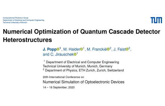
D03–Numerical Optimization of Quantum Cascade Detector Heterostructures
We demonstrate a Bayesian optimization framework for quantum cascade (QC) devices in the mid-infrared (mid-IR) and terahertz (THz) regime. The optimization algorithm is based on Gaussian process regression (GPR) and the devices are evaluated using a perturbed rate equation approach based on scattering rates calculated self-consistently by Fermi’s golden rule or alternatively extracted from an […]
SC10–Plasmonic enhancement of light-harvesting efficiency in Perovskite solar cells embedding Ag nanorods
Perovskite solar cells have attracted great attention in recent years due to its advantageous features including low production cost. Incorporation of plasmonic metal nanocrystals is a promising approach for broadening and enhancing the light harvesting of Perovskite solar cells. In this paper, we report a facile and versatile route to tune the photoresponse of perovskite […]
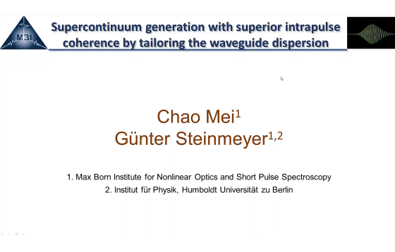
PD08–Supercontinuum generation with superior intrapulsecoherence in dispersion-tailored waveguides
Intrapulse coherence is an important performance metric for applications of supercontinua, including precision frequency metrology and attosecond science. These applications require a stable carrier-envelope phase, which is usually measured by f–2f interferometry. Here, the potential for superior intrapulse coherence with 100 and 400-fs input pulses is studied, exploiting different dispersion profiles. The simulation results in […]
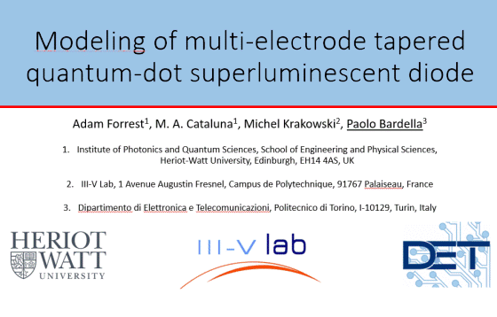
LED03–Modeling of multi-electrode tapered quantum-dot superluminescent diode
We introduce a rate equation based numerical model suitable for the description of the wide spectral asymmetry experimentally observed at the two facets of multi-electrode tapered superluminescent diode based on Quantum Dot material. Numerical simulations carried out with this model were able to quantitatively reproduce the behavior of a two-section SLD and explain the reported […]
MM02–Connecting numerical simulation and machine learning: How to bridge the gap between theory and reality?
Machine learning and numerical simulation represent opposite approaches to computational analysis of the real world, inductive vs. deductive. However, both methods suffer from various uncertainties and even their combination often fails to link theory and reality. This paper presents a critical review of such connections and proposes improvement options for optoelectronic devices.
LD04–Modeling Tunnel Junctions for VCSELs: A Self-Consistent NEGF-DD Approach
In this work we investigate carrier transport in tunnel junctions for vertical-cavity surface-emitting lasers by a novel self-consistent simulation framework for semiconductor quantum devices. Based on a Poisson-drift-diffusion foundation, in this approach quantum features are described through a nonequilibrium Green’s function formalism. The simulator is validated through a comparison with experimental results.
NM01–Ferrimagnetic garnets for integrated non-reciprocal devices
Ferrimagnetic garnets are promising materials for applications in integrated non-reciprocal devices due to their low optical absorption and relatively large magneto-optical response at telecommunication wavelengths. However, their implementation into phonotic chips is rather difficult due to large lattice parameters and thermal expansion mismatch with common photonic substrates. In this talk, we present our latest progress […]
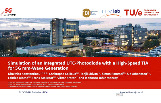
D04– Simulation of an Integrated UTC-Photodiode with a High-Speed TIA for 5G mm-Wave Generation
This work introduces a subsystem level cosimulation for generation, boosting and transmission of millimeter wave signals for 5G applications. The simulation processes to model the full equivalent circuit of uni-traveling carrier photodiodes based on reflection coefficient measurements are analyzed. The optoelectronic lumped equivalent is co-integrated with a transimpedance amplifier design synthesized by high speed transistors. […]
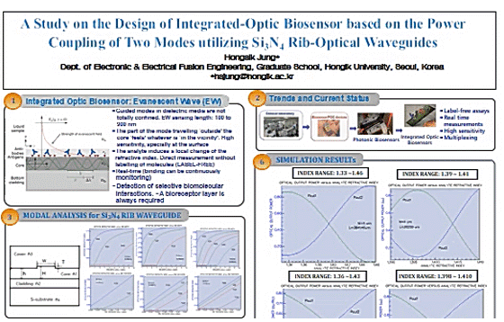
PD06–A Study on the Design of Integrated-Optic Biosensor based on the Power Coupling of Two Modes utilizing Si3N4 Rib-Optical Waveguides
We proposed an integrated-optical biosensor configuration that operates at a wavelength of 0.63 μm based on the evanescent-wave and lateral two-mode power coupling of Si3N4 rib-optical waveguides formed on a Si/SiO2/Si3N4/SiO2 multilayer thin films. The coupling between the two propagating modes in the sensing region produces a periodically repeated optical power exchange along the propagation. […]
PD09–Reflection Spectra Analysis and Optimization of Phase-modulated Waveguide-grating Reflectors
Phase-modulated waveguide gratings are promising reflective optical elements for widely tunable laser applications. We present an analysis on their comb-like reflectivity response and address the impact of phase-shifts on the number of large reflection peaks, their envelope and on the effective grating coefficient. Utilizing a robust phase-modulation approach, this paper shows a quasi-stochastic numerical optimization […]
LED01–Optical resolution of light engine based on InGaN/GaN nanoLED arrays: toward a superresolved light source
We present the optical simulations of a novel illumination source based on nanoLED arrays for the possible application in superresolved microscopy. We are simulating the images of various gold nanoparticle arrangements collected by the proposed nanoillumination microscope. The images are then analysed in order to understand the capabilities and limitations of the microscope.
N01–Quantum corrections to the efficiency of solar cells with conductive nanostructured layers
It was shown in many experiments that the incorporation of metallic nanostructures into photovoltaic devices results in the enhancement of solar cell efficiency. Most simulations of such devices are based on classical electrodynamics and neglect quantum effects arising from nanosized metallic structures. Here, we look at nonlocal electron-electron interactions, Lorentz friction and strong coupling of […]
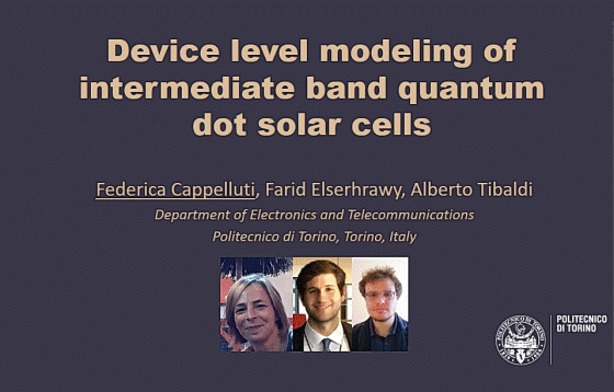
SC01–Device level modeling of intermediate band quantum dot solar cells
Among many material candidates for next-generation solar cells, quantum dots offer unique opportunities. Aiming to maximally harness their nanoscale bandgap engineering, in this work we outline a multiscale, multiphysics modeling approach for the device level simulation of quantum dot solar cells. Examples of experimental validation are discussed, emphasizing the potential of light trapping techniques towards […]
D09–Efficient Absorption Enhancement Approaches for AlInAsSb Avalanche Photodiodes for 2-μm Applications
We describe two photon-trapping structures to enhance the quantum efficiency of AlInAsSb APDs for 2-μm detection. Finite-difference time-domain (FDTD) simulations show the absorption can be enhanced by more than 100 % with a triangular lattice photonic crystal, and nearly 400 % by applying a metal grating, for normal incidence at 2 µm.
D06–Scaling Effects on the Plasmonic Enhancement of Butt-Coupled Waveguide Photodetectors
We employed 3D opto-electrical simulations to study the scaling effects of a plasmonic structure on the optical performance of butt-coupled waveguide photodetectors by placing an Ag stripe on top of the intrinsic region. It is found that cut-offs which are limited by carrier drift in the high-field region of the non-plasmonic device improve with longer […]
PD05–Design of a Broadband Integrated Notch Filter in Silicon Nitride
A broadband integrated notch filter, using the silicon nitride (Si3N4) platform, is presented. It achieves an extinction ratio (ER) of 60 dB and a full width at half maximum (FWHM) of 10 nm at the central wavelength (CW) 785 nm. The main filter components are Bragg gratings (BGs). For separating the occurring reflections from the […]
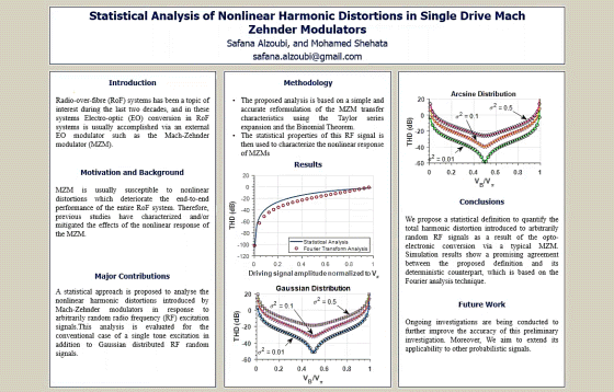
PD10–Statistical Analysis of Nonlinear Harmonic Distortions in Single Drive Mach Zhender Modulators
In this preliminary investigation, a statistical approach is proposed to analyze the nonlinear harmonic distortions introduced by Mach-Zehnder modulators (MZMs) in response to arbitrarily random radio frequency (RF) excitation signals. The proposed analysis is based on a simple and accurate reformulation of the MZM transfer characteristics using the Taylor series expansion and the Binomial Theorem. […]
LD01–Third Order Dispersion in Optical Time Delayed Systems: The case of Mode-Locked Vertical External-Cavity Surface-Emitting Lasers
Time-delayed dynamical systems materialize in situations where distant, point-wise, nonlinear nodes exchange information that propagates at a finite speed. However, they are considered devoid of dispersive effects, which are known to play a leading role in pattern formation and wave dynamics. We show how dispersion may appear naturally in delayed systems and we exemplify our […]
N02–Nucleation chronology and electronic properties of In(As,Sb,P) graded-composition quantum dots
We have studied nucleation process and electronic properties of graded-composition quantum dots(GCQDs) grown from In-As-Sb-P in the liquid phase for application in mid-infrared devices like photoresistors or photoconductive cells. The GCQD ensemble exhibits diameters of 10 – 120 nm and heights of 2 – 20 nm. Compositional grading is a typical feature of quantum dots […]
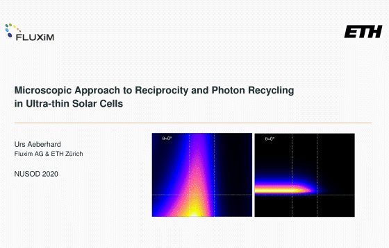
SC03–Microscopic approach to reciprocity and photon recycling in ultrathin solar cells
In contrast to their bulk counterparts, ultrathin solar cells exhibit bias-dependent optical properties. This has severe implications for the validity of conventional opto-electronic reciprocity relations. We review the predictions of this phenomenon from quantum-kinetic theory and discuss the experimental confirmation, as well as the extension of the theoretical framework for the rigorous assessment of photon […]
NM09–A fiber optic probe for thermal therapy
We demonstrate a novel fiber optic device for controlled generation of photothermal effects. The fiber probe is pumped by a laser diode and incorporates polymer composites allowing to generate highly localized heat and obtain temperature measurements simultaneously. We analyze the temperature field in the vicinity of the device through computer simulations and these are validated […]
D07–Numerical simulation on the dependence of carrier transport characteristics on the thickness of the absorbing layer for GaAs-based blocked impurity band (BIB) terahertz detectors
The dependence of carrier transport characteristics on the thickness of the absorbing layer for Gallium Arsenide (GaAs) blocked-impurity-band (BIB) terahertz detector has been investigated in detail. It is found that responsivity linearly increases with the increased thickness of absorbing layer first, and after achieving a peak value, and then starts to dropping slowly.
PD04–Towards an efficient simulation framework for plasmonic organic hybrid E/O modulators
Due to the large computational resources required, with CPU times of the order of several days, full-wave optical simulators can be hardly exploited for the modeling and optimization of plasmonic organic hybrid electro/optic modulators. With the aim to drastically reduce such complexity, in this work we present a divide-et-impera strategy reducing the number of FDTD […]
PD11–Tunable Polarization Splitter Based on Asymmetric Dual-core Liquid Photonic Crystal Fiber
An asymmetric dual core photonic crystal fiber (ADC-PCF) tunable polarization splitter is reported and analyzed. The left core of the DC-PCF is infiltrated with nematic liquid crystal (NLC) material to control the wavelength at which coupling occurs between the dual cores of the proposed structure. Moreover, the suggested design can be tuned to split out […]
LD02–A Functional Mapping for Passively Mode-Locked Semiconductor Lasers
We present a modern approach for the analysis of passively mode-locked semiconductor lasers that allows for efficient parameter sweeps and time jitter analysis. It permits accessing the ultra-low repetition rate regime where pulses become localized states. The analysis including slow (e.g. thermal) processes or transverse, diffractive dynamics becomes feasible. Our method bridges the divide between […]
N03–A Bi quantum film potential as an inverse problem
Experiments generally only offer access to certain output parameters or spectra. When performing device simulations, we often assume that agreement of theoretical and experimental output means that the model describes the device well. However, this conclusion is by no means mandatory. Here, we show an example of a Bi quantum film where measurements show equidistant […]

